An ultra-low-noise, fast-switching microwave signal generator covering a continuous range from 100 kHz (8 kHz with option) up to 12.75, 20, 26, or 40 GHz, with sub-0.001 Hz resolution, accurately levelled output power, and high spurious suppression.
Model 865B · 8 kHz to 12.75 / 20 / 26 / 40 GHz · Data Sheet V146 · dc-50604202
1Introduction
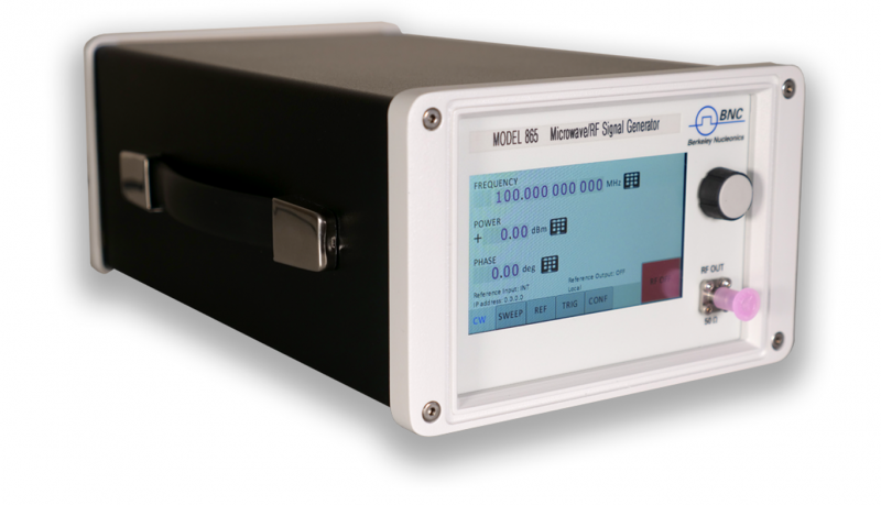
Ultra-Low Noise Microwave Signal Generator, 8 kHz to 12.75, 20, 26 and 40 GHz
The Model 865B is an ultra-low-noise and fast-switching microwave signal generator covering a continuous frequency range from 100 kHz (8 kHz with option) up to 12.75, 20 GHz, 26 or 40 GHz, respectively, with a lower than 0.001 Hz resolution.
The Model 865B provides an accurately levelled output power range and high spurious suppression. Advanced frequency synthesis combines the fastest switching speed with ultra-low SSB phase noise and fine frequency and power resolution.
The 865B supports analog AM, FM, PM modulation, as well as frequency chirps and pulse modulation with programmable patterns and narrow pulses.
The 865B allows for fast digital sweeps including flexible list sweeps, where frequency, power and dwell times can be set individually. A flexible triggering system simplifies synchronization within test environments.
All 865B models operate with ultra-stable temperature compensated frequency reference (OCXO) to ensure minimal drift and can be phase-locked to an external reference.
The compact unit allows for full front panel control via touch panel display. It can also be intuitively controlled by a PC based GUI Software. Moreover, the instrument offers various communication interfaces like USB, LAN or GPIB. Each interface allows for easy and fast communication using SCPI 1999 command set. Remote control of the instrument can be quickly attained from any host system. A customer-supplied application programming interface (API) or programming examples for Matlab, Labview, C++ and other commercially available tools make the control implementation very straightforward.
Definitions
The specifications in the following pages describe the warranted performance of the instrument for 23 ±5 °C after a 30-minute warm-up period.
Typical: Expected mean values, not warranted performance.
Min and Max: Parameter range that is guaranteed by product design, and/or production tested. Warranted performance specifications include guard-bands to account for the expected statistical performance distribution, measurement uncertainties, and changes in performance due to environmental conditions.
Applications
Ideal ADC clock (analog-to-digital converter)
Lowest close-in low phase (with Option LN)
Radar receiver testing
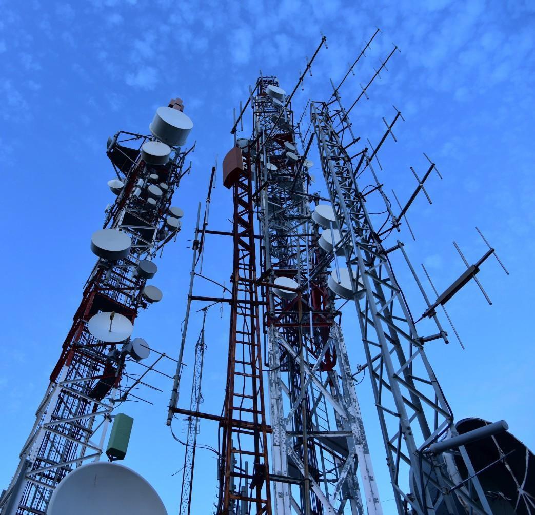
Communications and broadcast infrastructure.Satellite and SATCOM systems.Radar receiver test.
2Available Options
The following options can be ordered to extend or enhance the 865B. See Ordering Information for the full option list and model combinations.
Option
Description
LN
Enhanced close in phase noise & frequency stability.
LN+
Enhanced close in phase noise & further enhanced long term frequency stability.
FS
Ultra-fast switching speed.
NP
Narrow pulse modulation.
NEC
Narrow pulse modulation / fast switching (see specifications).
MOD
Analog modulation (AM, FM, PM, pulse).
FILT
Harmonic filtering (not in combination with option PE4).
8K
Frequency range extension to 8 kHz.
VREF
Variable external reference.
PE / PE2 / PE4
Electrical or mechanical step attenuators (level extension). See Ordering Information for model-specific ranges.
3Frequency Parameters / Range
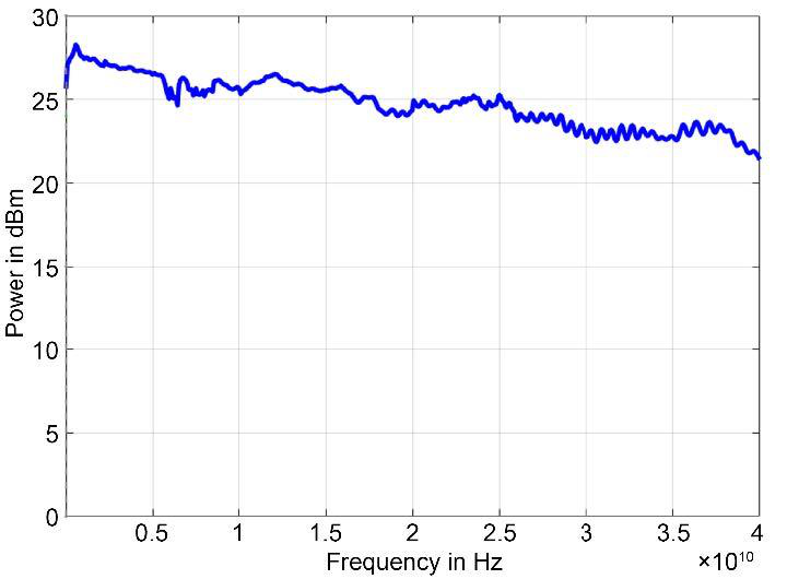
See Figures 5 to 8 (maximum output power vs. frequency) in Level Performance.
Parameter
Min
Typical
Max
Note
Frequency Range
100 kHz
12.75 GHz
865B-12
100 kHz
20 GHz
865B-20
100 kHz
26 GHz
865B-26
100 kHz
40 GHz
865B-40
8 kHz
Fmax
Option 8K
Resolution
0.001 Hz
Phase Resolution
0.01 deg
Switching Speed
1.5 ms (SCPI CW mode)
Valid signal after SCPI received.
500 µs (Sweep / List Mode)
30 µs
Option FS
See sweep
Option NEC
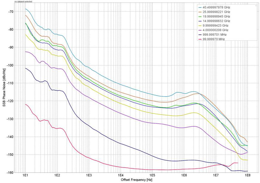
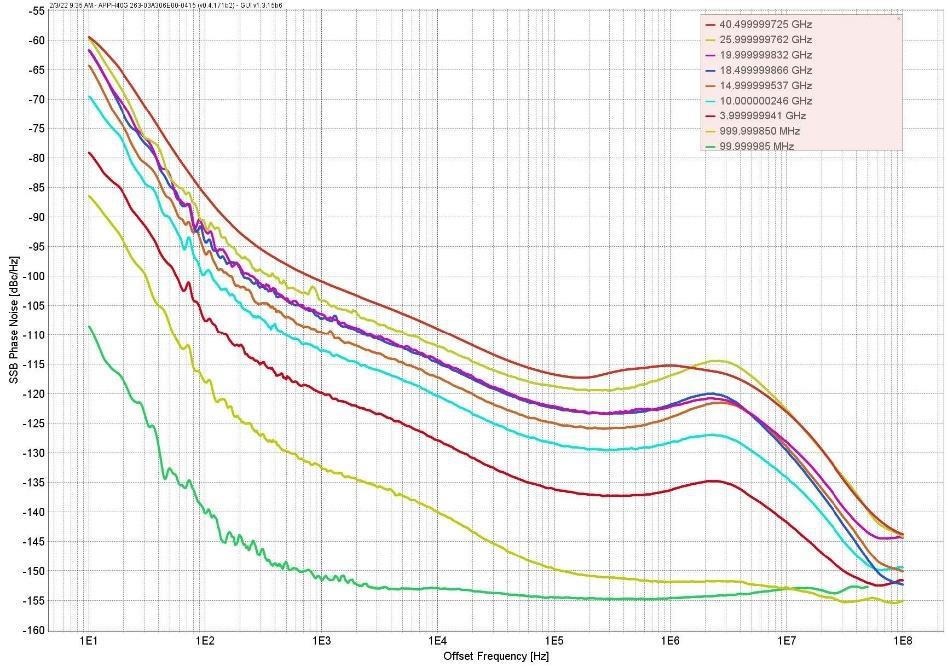
4Phase Noise
Figure 1: SSB Phase Noise Performance with option LN.Figure 2: SSB Phase Noise Performance, without option LN.
Parameter
Min
Typical
Max
Note
SSB Phase noise at 1 GHz (See also plots / tables)
At 10 Hz from carrier
-87 dBc/Hz
-100 dBc/Hz
-86 dBc/Hz
Option LN
At 1 kHz from carrier
-130 dBc/Hz
-125 dBc/Hz
At 100 kHz from carrier
-148 dBc/Hz
-144 dBc/Hz
SSB Phase noise at 4 GHz
At 10 Hz from carrier
-74 dBc/Hz
-68 dBc/Hz
-86 dBc/Hz
-74 dBc/Hz
Option LN
At 1 kHz from carrier
-118 dBc/Hz
-114 dBc/Hz
At 100 kHz from carrier
-136 dBc/Hz
-132 dBc/Hz
SSB Phase noise at 10 GHz
At 10 Hz from carrier
-67 dBc/Hz
-60 dBc/Hz
-78 dBc/Hz
-66 dBc/Hz
Option LN
At 1 kHz from carrier
-108 dBc/Hz
-104 dBc/Hz
At 100 kHz from carrier
-127 dBc/Hz
-123 dBc/Hz
SSB Phase noise at 40 GHz
At 10 Hz from carrier
-55 dBc/Hz
-48 dBc/Hz
-66 dBc/Hz
-53 dBc/Hz
Option LN
At 1 kHz from carrier
-96 dBc/Hz
-92 dBc/Hz
At 100 kHz from carrier
-115 dBc/Hz
-111 dBc/Hz
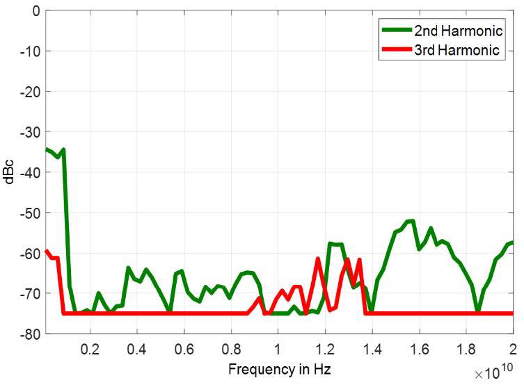
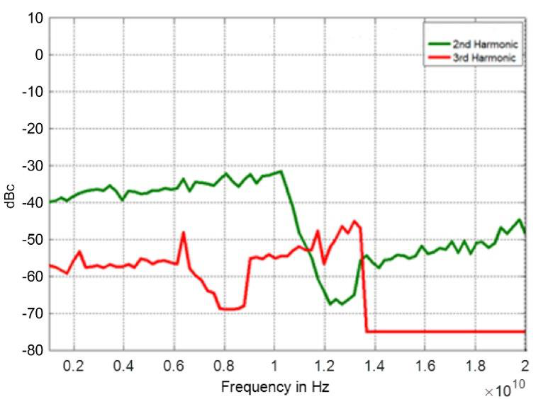
5Spectral Purity
Figure 3: Harmonics (2nd, 3rd at P=+5 dBm, 865B-40 with option FILT).Figure 4: Harmonics (2nd, 3rd at P=5 dBm, 865B-20).
Parameter
Min
Typical
Max
Note
Harmonics (at 0 dBm Pout)
0.01 to 6 GHz
-40 dBc
-30 dBc
>6 GHz
-35 dBc
-30 dBc
>10.5 GHz
-55 dBc
-45 dBc
865B-12/20
-30 dBc
-25 dBc
865B-26/40
Option FILT, >20 GHz
-60 dBc
-48 dBc
All models, see plots
Sub-harmonics
<5 GHz
-75 dBc
-65 dBc
5 - 20 GHz
-70 dBc
-60 dBc
>20 GHz
-55 dBc
-50 dBc
Option FILT, >20 GHz
-65 dBc
-55 dBc
Non-harmonic spurious (> 10 kHz offset)
<1.2 GHz
-90 dBc
-60 dBc
1.2 - 2.5 GHz
-92 dBc
-60 dBc
2.5 - 5 GHz
-90 dBc
-58 dBc
5 - 10 GHz
-84 dBc
-58 dBc
10 - 20 GHz
-80 dBc
-58 dBc
>20 GHz
-70 dBc
-50 dBc
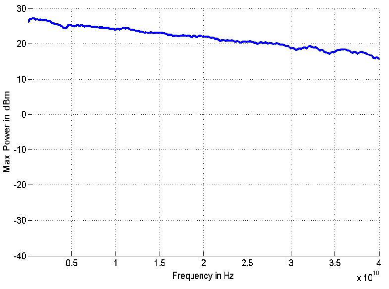
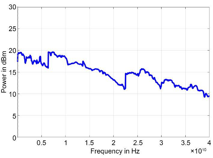
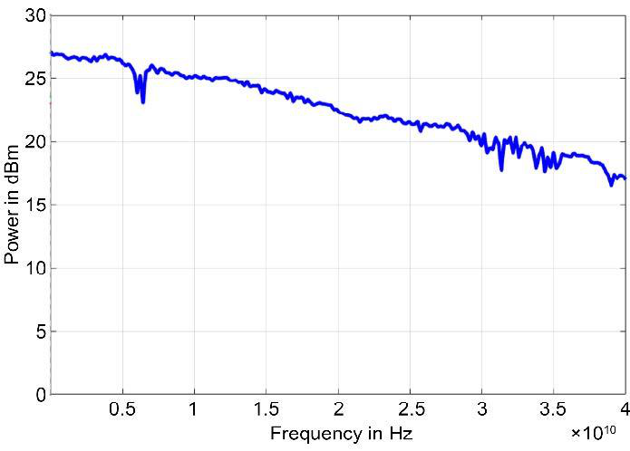
6Level Performance
Figure 5: Maximum Output Power 0.01 to 40 GHz.Figure 6: Max Output Power 0.01 to 40 GHz (865B-40 with option PE4).Figure 7: Max Output Power 0.01 to 40 GHz (with option FILT+PE2).Figure 8: Max Output Power 0.01 to 40 GHz (with option PE/PE2).
Parameter
Min
Typical
Max
Note
Output Power Range (865B-12/20)
8 to 100 kHz
-25 dBm
+15 dBm
Option 8K
0.1 to 10 MHz
-25 dBm
+24 dBm
0.01 to 5 GHz
-25 dBm
+26 dBm
5 to 12.75 GHz
-25 dBm
+24 dBm
12.75 to 18 GHz
-25 dBm
+22 dBm
18 to 20 GHz
-25 dBm
+20 dBm
Output Power Range (865B-12/20 with mechanical step attenuator, option PE)
0.1 to 10 MHz
-90 dBm
+23 dBm
0.01 to 5 GHz
-90 dBm
+25 dBm
5 to 12.75 GHz
-90 dBm
+23 dBm
12.75 to 18 GHz
-90 dBm
+19 dBm
18 to 20 GHz
-90 dBm
+17 dBm
Output Power Range (865B-12/20 with mechanical step attenuator, option PE2)
0.1 to 10 MHz
-120 dBm
+23 dBm
0.01 to 6 GHz
-120 dBm
+24 dBm
6 to 12.75 GHz
-120 dBm
+21 dBm
12.75 to 20 GHz
-120 dBm
+19 dBm
18 to 20 GHz
-120 dBm
+17 dBm
Output Power Range (865B-40)
8 to 100 kHz
-25 dBm
+15 dBm
Option 8K
0.1 to 10 MHz
-25 dBm
+24 dBm
0.01 to 6 GHz
-25 dBm
+25 dBm
6 to 12.75 GHz
-25 dBm
+24 dBm
12.75 to 26 GHz
-25 dBm
+21 dBm
26 to 40 GHz
-25 dBm
+18 dBm
See plot
Output Power Range (865B-40 with electrical step attenuator, option PE4)
0.1 to 10 MHz
-55 dBm
+23 dBm
0.01 to 6 GHz
-55 dBm
+24 dBm
6 to 12.75 GHz
-55 dBm
+22 dBm
12.75 to 20 GHz
-55 dBm
+20 dBm
20 to 30 GHz
-55 dBm
+17 dBm
30 to 40 GHz
-55 dBm
+14 dBm
See plot
Output Power Range (865B-40 with mechanical step attenuator, option PE)
0.1 to 10 MHz
-90 dBm
+24 dBm
0.01 to 6 GHz
-90 dBm
+24 dBm
6 to 12.75 GHz
-90 dBm
+22 dBm
12.75 to 20 GHz
-90 dBm
+21 dBm
20 to 30 GHz
-90 dBm
+18 dBm
30 to 35 GHz
-90 dBm
+17 dBm
35 to 40 GHz
-90 dBm
+16 dBm
Output Power Range (865B-40 with mechanical step attenuator, option PE2)
0.1 to 10 MHz
-120 dBm
+23 dBm
0.01 to 6 GHz
-120 dBm
+24 dBm
6 to 12.75 GHz
-120 dBm
+21 dBm
12.75 to 20 GHz
-120 dBm
+21 dBm
20 to 30 GHz
-120 dBm
+17 dBm
30 to 35 GHz
-120 dBm
+16 dBm
35 to 40 GHz
-120 dBm
+15 dBm
See plot
Output Power Range (all 865B with option FILT)
0.1 to 10 MHz
-25 dBm
+15 dBm
0.01 to 20 GHz
-25 dBm
+13 dBm
20 to 40 GHz
-25 dBm
+10 dBm
See plot
Output Power Range (all 865B with option FILT, PE/PE2)
0.1 to 10 MHz
-120 dBm
+15 dBm
0.01 to 20 GHz
-120 dBm
+13 dBm
20 to 35 GHz
-120 dBm
+10 dBm
35 to 40 GHz
-120 dBm
+6 dBm
See plot
Power Resolution
0.01 dB
Note: Figure 9 (Max Output Power 8 kHz to 100 kHz, with option 8K) is listed in the source datasheet as "to be added" and is not yet available.
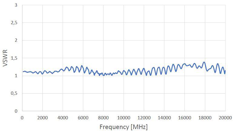
7Reverse Power Protection and Output Impedance
Figure 10: Typical VSWR (865B-20).
Parameter
Min
Typical
Max
Note
Reverse Power Protection
DC Voltage
±10 V
RF Power
30 dBm
Output Impedance
Output impedance
50 Ohms
VSWR
1.4
1.9
8Power Level Uncertainty
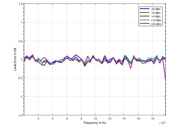
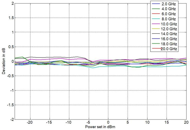
Figure 11: Typical Frequency Response 0 to 20 GHz at different power levels (865B-20).Figure 12: Typical Output Power Linearity (865B-20).
Values shown are Min/Max; the value in parentheses is the Typical Value.
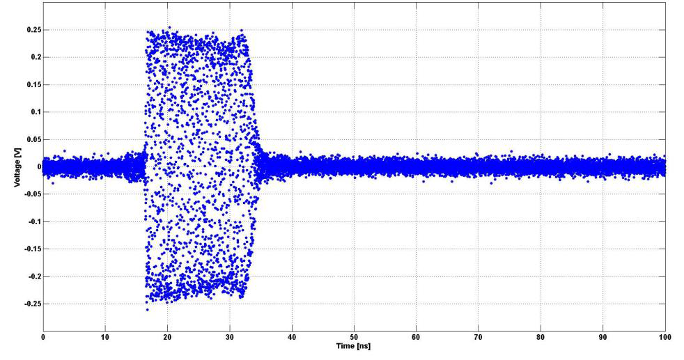
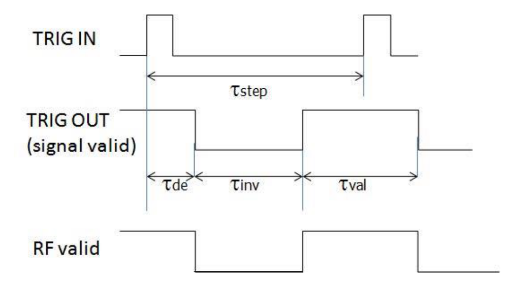
TRIGGER OUT Synchronization mode for multiple sources
Modes
Trigger on sweep start, Trigger on each point, Signal valid
18GUI
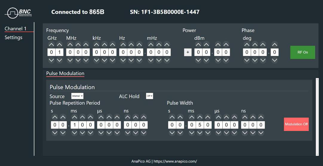
Figure 16: Desktop App GUI.Figure 17: Web Browser GUI.
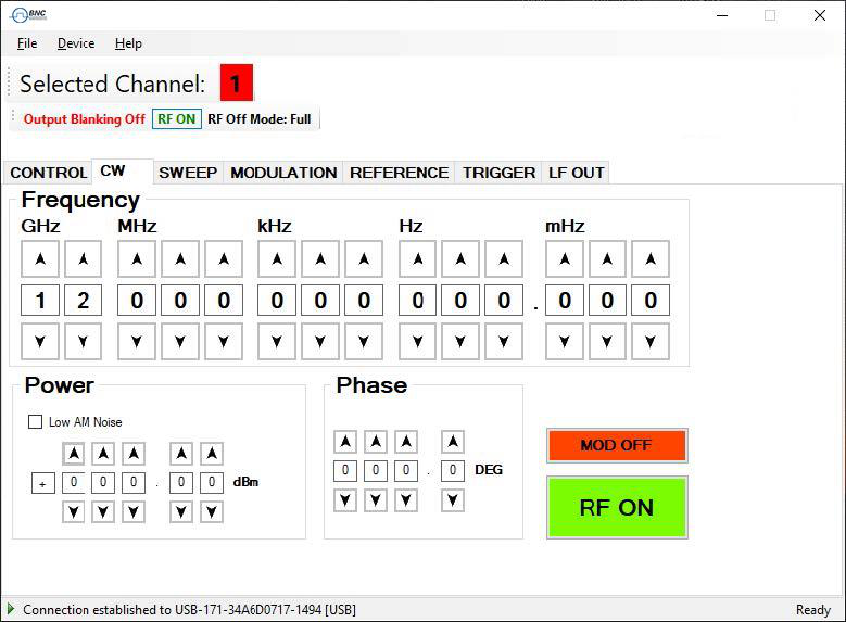
The 865B can be operated from the full front panel touch display, from the PC-based Desktop App GUI, or from a Web Browser GUI served by the instrument. The desktop and web applications expose control of CW frequency, power, phase, sweep, modulation, reference, and trigger functions.
19Connectors
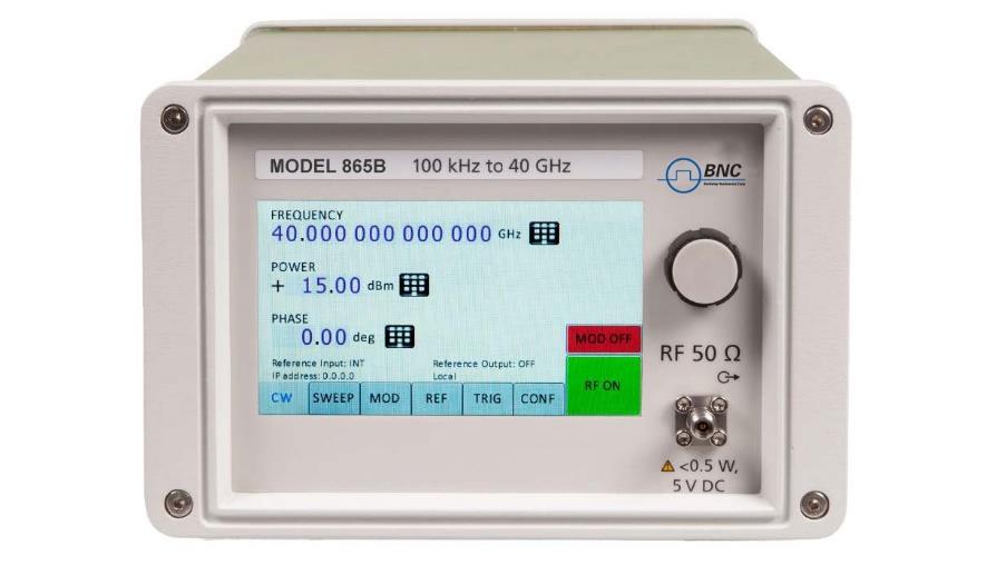
Front Panel
Color touch display
RF output
865B-40: K (2.92 mm) female
865B-12, 20, 26: SMA female
Rotary knob
Model 865B front panel: color touch display, RF output (50 Ω), and rotary knob.
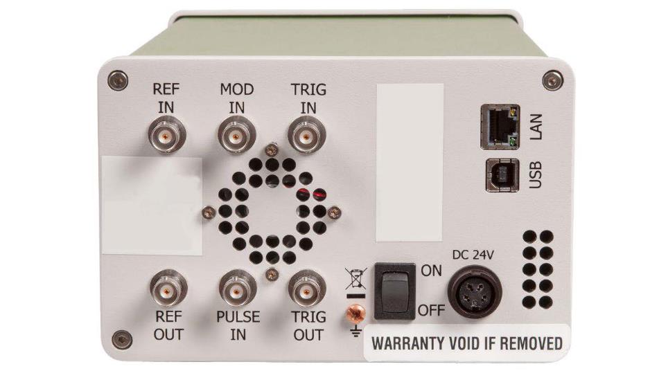
Rear Panel
TRIG IN: Trigger input: BNC female
TRIG OUT: Trigger output: BNC female
REF OUT: Internal reference output: BNC female
REF IN: External reference output: BNC female
MOD IN: Modulation input for FM/PM: BNC female
PULSE IN: Pulse modulation input: BNC female
LAN connection: RJ-45
USB 2.0 host and device
GPIB: IEEE-488.2, 1987 with listen and talk
DC Power plug (24 V, 3 A)
DC power switch
Model 865B rear panel showing REF IN, MOD IN, TRIG IN, REF OUT, PULSE IN, TRIG OUT, LAN, USB, and DC 24 V power connectors.
20Ordering Information
Host Model
Product
Description
865B-12
865B-12
100 kHz - 12.75 GHz
865B-20
865B-20
100 kHz - 20 GHz
865B-26
865B-26
100 kHz - 26 GHz
865B-40
865B-40
100 kHz - 40 GHz
865B-XX
Option LN
Enhanced close in phase noise & frequency stability
865B-XX
Option LN+
Enhanced close in phase noise & further enhanced long term frequency stability
865B-XX
Option FS
Ultra-fast switching speed
865B-XX
Option NP
Narrow pulse modulation
865B-XX
Option MOD
Analog modulation
865B-XX
Option FILT
Harmonic filtering (not in combination with option PE4)
865B-XX
Option 8K
Frequency range extension to 8 kHz
865B-XX
Option VREF
Variable external reference
865B-12/20/26
Option PE4-12/20226
Electrical step attenuator (12, 20 & 26 GHz version) (not in combination with option FILT)
865B-40
Option PE4-40
Electrical step attenuator (40 GHz version) (not in combination with option FILT)
865B-12/20
Option PE-12/20
Mechanical step attenuator down to -90 dBm (12 & 20 GHz version)
865B-26/40
Option PE-26/40
Mechanical step attenuator down to -90 dBm (26 & 40 GHz version)
865B-12/20/26
Option PE2-12/20/26
Mechanical step attenuator down to -120 dBm (12, 20 & 26 GHz version)
865B-40
Option PE2-40
Mechanical step attenuator down to -120 dBm (40 GHz version)
865B-XX
Option EB
External power bank adapter cable
865B-XX
Option GPIB
GPIB interface
865B-XX
Option RM
19" 3U rack-mount kit
865B-XX
Option 1URM
19" 1U rack-mount module
865B-XX
Option REAR
Move output to rear panel
865B-XX
Option FLASH
MicroSD card slot for removable SD memory
865B-XX
Option IEC
IEC 17025 calibration with certificate
865B-XX
Option Bag
Portable bag
865B-XX
Option Retrofit
Applies when options are back-ordered
21General Characteristics
Remote programming interfaces
Ethernet 100BaseT LAN interface
USB 2.0 host & device
GPIB (IEEE-488.2,1987) with listen and talk (optional)
Control language SCPI Version 1999.0
Parameter
Specification
Power requirements
24V ± 3.0 VDC; 25 W maximum
AC adapter supplied
100-240 VAC in/ 24 V 4.0 A DC out
Environmental
Levels similar to MIL-PRF-28800F Class 3/4. Samples of this product have been type-tested to be robust under the environmental conditions of storage, transportation, and end-use with different temperature, humidity, shock, vibration, altitude, and power line conditions.
Operating temperature range
0 to 45 °C
Storage temperature range
-40 to 70 °C
Operating and storage altitude
up to 15,000 feet (4600 m)
EMC
Complies and EMC regulations and directives for emission and immunity to interference (EN 61326-1 Industrial, EN/IEC 61326-2-1).
Safety
Complies with applicable Safety regulation in line with IEC/EN 61010-1. This product complies with directive 2011/65/EU.
Weight
6 lbs (2.5 kg) net, ≤ 9 lb (4 kg) with ship-ready package
Dimensions
4.21 in H x 6.77 in W x 11.42 in L / 106 mm H x 172 mm W x 290 mm L, incl. connectors
Recommended calibration cycle
24 months
Compliance. EMC complies with EMC regulations and directives for emission and immunity to interference (EN 61326-1 Industrial, EN/IEC 61326-2-1). Safety complies with applicable safety regulation in line with IEC/EN 61010-1. This product complies with directive 2011/65/EU. The 865B carries the CE mark shown.