1Overview
The Berkeley Nucleonics Model 685 is a high-performance arbitrary waveform generator that pairs a 6.16 GS/s sample rate (12.32 GS/s in RF mode) with 16-bit vertical resolution and output frequency up to 6 GHz. It is available with 2, 4, or 8 analog channels, with up to 4 Gpts of waveform memory per channel and up to 32 synchronized digital channels for mixed-signal generation. The instrument also operates as a Serial Pattern Generator (SPG) and Digital Pattern Generator.
Features
- 2, 4 or 8 analog channels
- 6.16 GS/s (12.32 GS/s in RF mode)
- 16-bit vertical resolution
- Up to 6 GHz output frequency
- < 110 ps rise/fall time
- Up to 5 Vpp output voltage and ± 2.5 V hardware offset into 50 Ω
- Up to 4 Gpts waveform memory per channel
- Up to 32 digital channels synchronous with analog generation
Applications
- Aerospace and Defense
- Institute and University Research
- Semiconductor Tests
- Automotive
- IoT
2Features & Benefits
- Sample rate can be programmed from 1 S/s to 6.16 GS/s (12.32 GS/s in RF mode), with 16-bit vertical resolution, ensuring exceptional signal integrity.
- Arbitrary waveform memory up to 4 Gpts for each analog channel.
- Mixed Signal Generation: 2, 4, or 8 analog channels with 8, 16, or 32 synchronized digital channels for debugging and validating digital design.
- Three operation modes: Simple Rider AFG (DDS AFG mode), True Arb (variable clock Arbitrary AWG mode) and SPG (Serial Pattern Generator).
- Digital outputs provide up to 1.54 Gb/s data rate in LVDS format. LVDS to LVTTL adapter is available.
- Advanced sequencer with up to 16384 user-defined waveforms provides the possibility of generating complex signal scenarios with the most efficient memory usage.
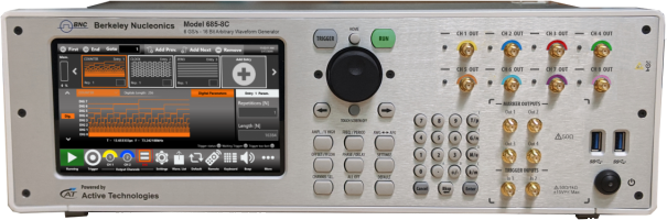
- Windows-based platform with 7 in touchscreen, front panel buttons and knob.
- Compact form factor, convenient for bench top and fully fit with 3U, 19" rack-mount standard.
- LAN, USB-TMC and GPIB interfaces for remote control.
3Model Configurations
The Model 685 is offered in single-ended (C) and differential (CD) variants with 2, 4, or 8 analog channels. Digital outputs and marker outputs scale with channel count.
| Model | Analog Channels | Output Type | Digital Out (optional) | Marker Out |
|---|---|---|---|---|
| 685-2C / 685-2CD | 2 | Single-ended (C) / Differential (CD) | 0 / 8 optional | 1 |
| 685-4C / 685-4CD | 4 | Single-ended (C) / Differential (CD) | 0 / 8 / 16 optional | 2 |
| 685-8C / 685-8CD | 8 | Single-ended (C) / Differential (CD) | 0 / 8 / 16 / 24 / 32 optional | 4 |
Up to 4 instruments can be synchronized to obtain a 32 analog / 128 digital channel generator. A dedicated synchronization bus guarantees intra-chassis synchronization.
4User Interface
Simple Rider AFG: Function Generator Mode
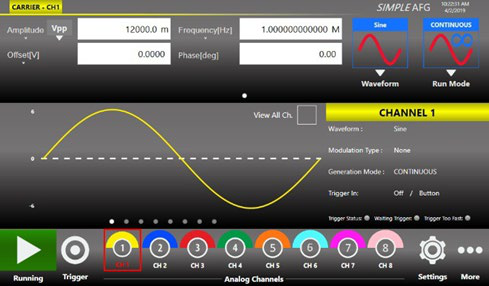
The Simple Rider AFG UI is designed using a touchscreen interface, developed to put all the capabilities of modern waveform generators at your fingertips. All instrument controls and parameters are accessible through an intuitive UI that recalls the simplicity of modern tablets and smartphones. Scientists and engineers can use gestures and touch commands to create advanced waveforms or digital patterns with ease.
- The swipe gesture gives easy access to the output waveform parameters.
- A touch-friendly virtual numeric keypad improves the user experience when entering data.
- Time-saving shortcuts and intuitive icons simplify the instrument setup.
Simple Rider TrueArb: AWG and DPG Mode
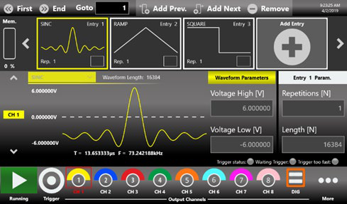
In the Simple Rider True-Arb interface, users can define complex waveforms with up to 16,384 sequence entries of analog waveforms and digital patterns, and define their execution flow by means of loops, jumps, and conditional branches. Digital output combined and synchronized with analog output signals is an ideal tool to troubleshoot and validate digital design. The waveform memory length of up to 4 GSamples on each channel, combined with up to 16,384 sequence entries and up to 4,294,967,294 repetitions, makes the Model 685 the ideal generator for the most demanding technical applications.
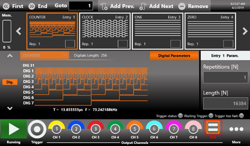
Thanks to the intuitive waveform sequencer user interface, you can create the most complex waveform scenarios with just a few screen touches. Model 685 supports the standard Ethernet interface for remote control and easy customized instrument programming.
Simple Rider SPG: Serial Pattern Generator Mode

The touchscreen display interface allows creating pattern scenarios in a few screen touches. The Data Pattern Generator provides the capability to generate PRBS patterns and up to 2 MSymbols custom patterns where bit transitions can have arbitrarily user-defined shapes. The Model 685 Serial Pattern Generator can generate patterns up to 1.5 Gbaud. The software architecture makes it possible to generate the patterns in different generation modalities and to modulate the patterns with internal or external signals to generate different noise effects (jitter, ripple, and similar).
5Applications
Automotive
Today's cars include highly sophisticated and electronically controlled units with sensitive electronic components. The Model 685 combines a 6.16 GSa/s sampling rate with a 16-bit vertical resolution. It represents an ideal and successful tool for addressing the new testing challenges in the automotive industry. It includes:
- EMI debugging, troubleshooting, and testing
- Electrical standards emulation up to 5 V
IoT and Ind 4.0 Perfect RF Modulator
The Model 685 is the iconic instrument for this application. It can emulate complex RF I/Q modulation for simulation and test of wireless devices or for work on the Internet of Things and Industry 4.0 applications. Engineers may import waveforms to emulate devices for test purposes and impose distortion on waveforms (such as noise) to test device compliance with standards.
Semiconductor Testing
Emulation of complex signals with the inclusion of noise or distortions can be an excellent way to provide Compliance Components Test to help semiconductor engineers. The fast edges and pulse generation can be used to provide characterization in fast power devices.
Research Applications
Research centers and universities are key users of the Model 685. Complex waveform and sophisticated pulse emulation based on variable edges or multilevel signals can be perfectly created. The combination of fast edge generation, excellent dynamic range, and easy-to-use user interface meets the needs of scientists and engineers working on Quantum Research or large experiments such as Accelerators, Tokamak, or synchrotrons, to emulate signals without creating specific test boards.
- Emulation of detectors
- Emulation of signal sources adding noise
- Generation/playback of real-world signals
- Emulation of long PRBS sequences
- Modulating and driving laser diodes
Aerospace and Defense
The Model 685 works perfectly with electronic warfare signals, such as those produced by radar or sonar systems. This generator can also be fitted into a modular system for radio or I/Q signal modulation. It can create pulses useful in pulse electron beams, X-ray sources, flash X-ray radiography, lightning pulse simulators, and high-power microwave modulators.
- Frequency response, intermodulation distortion and noise-figure measurements
- Phase Locked Loop (PLL) pull-in and hold-range characterization
- Radar base-band signals emulation
6General Specifications
| Parameter | Model 685-2C / 2CD | Model 685-4C / 4CD | Model 685-8C / 8CD |
|---|---|---|---|
| Operating Mode | AFG Mode / True Arb Mode / SPG Mode | ||
| Analog Channels | 2 | 4 | 8 |
| Digital Out | 0 / 8 optional | 0 / 8 / 16 optional | 0 / 8 / 16 / 24 / 32 optional |
| Marker Out | 1 | 2 | 4 |
Output Channels
| Parameter | Single-ended (685-2C / 4C / 8C) | Differential (685-2CD / 4CD / 8CD) |
|---|---|---|
| Output Type | Single ended DC coupled | Differential DC coupled |
| Output Impedance | Single-ended: 50 Ω | Single-ended: 50 Ω Differential: 100 Ω |
| Connectors | SMA on front panel | |
DC Amplitude
| Parameter | Single-ended | Differential |
|---|---|---|
| Amplitude Range | ±2.5 V (into 50 Ω) | ±0.75 V Se. (into 50 Ω) ±1.5 V Diff. (into 100 Ω) |
| Resolution | 100 µV (nom), 5 digits | |
| Amplitude Accuracy (guaranteed) | ±(1% of |setting| + 5 mV) | ±(0.5% of |setting| + 2 mV) |
DC Baseline Hardware Offset (Common mode offset)
| Parameter | Single-ended | Differential |
|---|---|---|
| Resolution | < 4 mV or 4 digits | |
| Range (50 Ω into 50 Ω) | -2.5 V to +2.5 V | -2 V to +2 V |
| Range (50 Ω into High Z load) | -2.5 V to +2.5 V | -4 V to +4 V |
| Accuracy (50 Ω into 50 Ω) (guaranteed) | ± (1% of |setting| + 5 mV) | |
| AC Accuracy (1 kHz sine wave, 0 V offset, > 5 mVp-p amplitude, 50 Ω load) (guaranteed) | ± (1% of setting [Vpp] + 5 mV) | |
7True Arb — Baseband Mode
| Parameter | Model 685-2C / 4C / 8C · 685-2CD / 4CD / 8CD | |
|---|---|---|
| Operating Mode | Variable clock (True Arbitrary), Baseband mode | |
| Sample Rate | 1 S/s to 6.16 GS/s | |
| Sin(x)/x | 2.72 GHz @ 6.16 GS/s | |
| Run Modes | Continuous, Triggered Continuous, Single/Burst, Stepped, Advanced | |
| Vertical Resolution | 16 bit | |
| Waveform Length | 128 to 2G samples per channel (up to 4G samples optional) | |
| Waveform Granularity | 1 if the entry length is > 416 samples 32 if entry length is ≥ 128 and ≤ 416 samples | |
| Sequence Length | 1 to 16384 | |
| Sequence Repeat Counter | 1 to 4294967294 or infinite | |
| Timer Range / Resolution | 20 ns to 1.39 seconds / ± 1 sampling clock cycle | |
| Analog Channel to Channels skew — Range | 0 to 2.63 µs | |
| Analog Channel to Channels skew — Resolution | 100 fs | |
| Analog Channel to Channels skew — Accuracy | ±(1% of setting + 20 ps) | |
| Initial skew | < 20 ps | |
| Parameter | Single-ended (685-2C / 4C / 8C) | Differential (685-2CD / 4CD / 8CD) |
|---|---|---|
| Calculated bandwidth (0.35 / rise or fall time) | ≥ 2 GHz | ≥ 2.2 GHz |
| SFDR @ 100 MHz (Fsa = 6 Gsa/s, measured across DC to Fs/2, excluding fsa - 2·fout and fsa - 3·fout and excluding harmonic) | < -80 dBc | < -90 dBc |
| SFDR (Fsa = 6.16 Gsa/s, measured across DC to Fs/2, excluding fsa - 2·fout and fsa - 3·fout and excluding harmonic) 1 | 1 µHz to ≤ 600 MHz: < -80 dBc 600 MHz to ≤ 1.5 GHz: < -75 dBc 1.5 GHz to ≤ 2 GHz: < -65 dBc 2 GHz to ≤ 3 GHz: < -55 dBc | 1 µHz to < 100 MHz: < -90 dBc 100 MHz to ≤ 600 MHz: < -82 dBc 600 MHz to ≤ 1.5 GHz: < -75 dBc 1.5 GHz to ≤ 2 GHz: < -70 dBc 2 GHz to ≤ 3 GHz: < -62 dBc |
| Rise/fall time (1 Vp-p single-ended 10% to 90%) | ≤ 175 ps | ≤ 155 ps |
| Rise/fall time (1 Vp-p single-ended 20% to 80%) | ≤ 110 ps | ≤ 100 ps |
| Overshoot (1 Vp-p single-ended) | < 5% | < 6% |
| Random jitter on clock pattern (rms, typical) | < 2 ps | |
1 For 685-2C/4C/8C models the SFDR is evaluated @ 2.5 Vpp single ended nominal output amplitude. For 685-2CD/4CD/8CD models the SFDR is evaluated @ 1.5 Vpp differential nominal output amplitude provided to the spectrum analyzer through a Minicircuit TC1-1-13M+ balun.
8True Arb — RF Mode
| Parameter | Model 685-2C / 4C / 8C · 685-2CD / 4CD / 8CD | |
|---|---|---|
| Operating Mode | Variable clock (True Arbitrary), RF mode | |
| Output Sample Rate | 8.5 GS/s to 12.32 GS/s | |
| Sin(x)/x | 5.04 GHz @ 12.32 GS/s | |
| RF Modulation | I/Q quadrature | |
| RF Carrier Count per Output Channel | Single Carrier (2 components I0, Q0 for channel) Double Carrier (4 components, I0, Q0 and I1, Q1 for channel) | |
| RF Carrier Frequency Range | 0 up to 6 GHz | |
| RF Carrier Frequency Resolution | 1 mHz | |
| RF Carrier Phase | Programmable | |
| I/Q Component Data Rate | 1/8 of the Output Sample rate | |
| I/Q Component Prescaler | 0 to 2^32 | |
| Run Modes | Continuous, Triggered Continuous, Single/Burst, Stepped, Advanced | |
| I/Q Component Vertical Resolution | 16 bit | |
| I/Q Component Waveform Length | 32M to 500M samples for component (up to 1G samples optional) | |
| I/Q Component Waveform Granularity | 1 if the entry length is > 104 samples 8 if entry length is ≥ 32 and ≤ 104 samples | |
| Sequence Length | 1 to 16384 | |
| Sequence Repeat Counter | 1 to 4294967294 or infinite | |
| Timer Range / Resolution | 20 ns to 1.39 seconds / ± 1 Component sampling clock cycle | |
| I/Q Component to Component skew — Range | 0 to [16200 · 8 / Output Sampling Clock] s | |
| I/Q Component to Component skew — Resolution | [8 / Output Sampling Clock] s | |
| I/Q Component to Component skew — Accuracy | ±(1% of setting + 20 ps) | |
| Initial Skew | < 20 ps | |
9AFG Mode
General Specifications
| Parameter | Single-ended (685-2C / 4C / 8C) | Differential (685-2CD / 4CD / 8CD) |
|---|---|---|
| Amplitude | 0 to 5 Vpp (into 50 Ω) | 0 to 3 Vpp Diff. (into 100 Ω) 0 to 1.5 Vpp Se. (into 50 Ω) |
| Resolution | 100 µV (nom), 5 digits | |
| Operating Mode | DDS mode | |
| Standard Waveforms | Sine, Square, Pulse, Ramp, more (Noise, DC, Sin(x)/x, Gaussian, Lorentz, Exponential Rise, Exponential Decay, Haversine) | |
| Run Modes | Continuous, modulation, sweep, burst | |
| Arbitrary Waveforms | Vertical resolution: 16-bit; Waveform length: 16,384 points | |
| Internal Trigger Timer — Range / Resolution / Accuracy | 10.4 ns to 88 s / 80 ps / ±(0.1% setting + 5 ps) | |
Sine Waves
| Parameter | Single-ended | Differential |
|---|---|---|
| Frequency Range Sine (50 Ω into 50 Ω) 2 | 1 µHz to ≤ 1 GHz: 5 Vpp 1 GHz to ≤ 2 GHz: 4 Vpp | 1 µHz to ≤ 2 GHz: 3 Vpp Diff. 1 µHz to ≤ 2 GHz: 1.5 Vpp Se. |
| Flatness (1 Vpp, relative to 1 kHz) | DC to 2 GHz: ±0.5 dB | DC to 2 GHz: ±0.5 dB (1 Vpp diff., relative to 1 kHz) |
| Harmonic Distortion (1 Vp-p) | 1 µHz to ≤ 20 kHz < -75 dBc 20 kHz to ≤ 400 MHz < -70 dBc 400 MHz to ≤ 1 GHz < -60 dBc 1 GHz to ≤ 2 GHz < -55 dBc | |
| Total Harmonic Distortion (1 Vp-p) | 10 Hz to 20 kHz < 0.05% | |
| Spurious (measured across DC to Fs/2) 3 | 1 µHz to ≤ 500 MHz: < -75 dBc 500 MHz to ≤ 1.5 GHz: < -70 dBc 1.5 GHz to ≤ 2 GHz: < -55 dBc | 1 µHz to ≤ 250 MHz: < -85 dBc 250 MHz to ≤ 500 MHz: < -80 dBc 500 MHz to ≤ 1.5 GHz: < -70 dBc 1.5 GHz to ≤ 2 GHz: < -60 dBc |
| Phase Noise (1 Vp-p, 10 kHz offset) | 20 MHz: < -127 dBc/Hz typ. 100 MHz: < -123 dBc/Hz typ. 1 GHz: < -105 dBc/Hz typ. | |
Square Waves
| Parameter | Value | |
|---|---|---|
| Frequency Range | 1 µHz to ≤ 770 MHz | |
| Rise/fall Time (10% to 90%) | 400 ps | |
| Rise/fall Time (20% to 80%) | 300 ps | |
| Overshoot (1 Vp-p) | < 2% | |
| Jitter (rms) | < 2 ps | |
Pulse Waves
| Parameter | Value | |
|---|---|---|
| Frequency Range | 1 µHz to ≤ 770 MHz | |
| Pulse Width | 500 ps to (Period – 500 ps) 4 | |
| Pulse Width Resolution | 20 ps or 15 digits | |
| Pulse Duty | 0.1% to 99.9% (limitations of pulse width apply) | |
| Leading/trailing edge transition time (10% to 90%) | 400 ps to 1000 s | |
| Leading/trailing edge transition time (20% to 80%) | 300 ps to 1000 s | |
| Transition Time Resolution | 2 ps or 15 digits | |
| Overshoot (1 Vp-p) | < 2% | |
| Jitter (rms, with rise and fall time ≥ 400 ps) | < 2 ps | |
Double Pulse Waves
| Parameter | Single-ended | Differential |
|---|---|---|
| Frequency Range | 1 µHz to ≤ 385 MHz: 10 Vpp where Vpp = |Vpp1| + |Vpp2| | 1 µHz to ≤ 385 MHz: 6 Vpp Diff. (1 µHz to ≤ 385 MHz: 3 Vpp Se) where Vpp = |Vpp1| + |Vpp2| |
| Other Pulse Parameters | Same as Pulse Waves | |
Ramp Waves
| Parameter | Value | |
|---|---|---|
| Frequency Range | 1 µHz to 75 MHz | |
| Linearity (< 10 kHz, 1 Vp-p, 100%) | ≤ 0.1% | |
| Symmetry | 0% to 100% | |
Other Waves
| Waveform | Frequency Range |
|---|---|
| Exponential Rise, Exponential Decay | 1 µHz to 75 MHz |
| Sin(x)/x, Gaussian, Lorentz, Haversine | 1 µHz to 150 MHz |
Additive Noise
| Parameter | Single-ended | Differential |
|---|---|---|
| Bandwidth (-3 dB) | 2 GHz | |
| Level | 0 V to 2.5 V - abs(carrier max value [Vpk]) | 0 V to 0.75 V Single Ended - abs(carrier max value [Vpk]) 0 V to 1.5 V Differential - abs(carrier max value [Vpk]) |
| Resolution | 1 mV | |
Arbitrary
| Parameter | Value | |
|---|---|---|
| Number of Samples | 2 to 16384 | |
| Frequency Range | 1 µHz to ≤ 770 MHz | |
| Analog Bandwidth (-3 dB) | 950 MHz | |
| Rise/Fall Time (10% to 90%) | 400 ps | |
| Rise/Fall Time (20% to 80%) | 300 ps | |
| Jitter (rms) | < 2 ps | |
Frequency Resolution & Accuracy
| Parameter | Value | |
|---|---|---|
| Frequency Resolution — Sine, Square, Pulse, Arbitrary, Sin(x)/x | 1 µHz or 15 digits | |
| Frequency Resolution — Gaussian, Lorentz, Exponential Rise, Exponential Decay, Haversine | 1 µHz or 14 digits | |
| Frequency Accuracy — Non-ARB | ± 2.0 ppm of setting | ± 500 ppb of setting (Opt.) | |
| Frequency Accuracy — ARB | ± 2.0 ppm of setting ±1 µHz | ± 500 ppb of setting ±1 µHz (Opt.) | |
2 Amplitude doubles on HiZ load. 3 For 685-2C/4C/8C models the spurious are evaluated @ 1 Vpp single ended nominal output amplitude. For 685-2CD/4CD/8CD models the SFDR is evaluated @ 1 Vpp differential nominal output amplitude provided to the spectrum analyzer through a Minicircuit TC1-1-13M+ balun. 4 Below 500 ps width, the pulse amplitude will have some reduction respect to the set value.
10Modulation
Amplitude Modulation (AM)
| Carrier Waveforms | Standard waveforms (except Pulse, DC and Noise), ARB |
| Modulation Source | Internal or external |
| Internal Modulating Waveforms | Sine, Square, Ramp, Noise, ARB |
| Modulating Frequency | Internal: 500 µHz to 61 MHz, External: 10 MHz maximum |
| Depth | 0.00% to 120.00% |
Frequency Modulation (FM)
| Carrier Waveforms | Standard waveforms (except Pulse, DC and Noise), ARB |
| Modulation Source | Internal or external |
| Internal Modulating Waveforms | Sine, Square, Ramp, Noise, ARB |
| Modulating Frequency | Internal: 500 µHz to 61 MHz, External: 10 MHz maximum |
| Peak Deviation | DC to 2 GHz |
Phase Modulation (PM)
| Carrier Waveforms | Standard waveforms (except Pulse, DC and Noise), ARB |
| Modulation Source | Internal or external |
| Internal Modulating Waveforms | Sine, Square, Ramp, Noise, ARB |
| Modulating Frequency | Internal: 500 µHz to 61 MHz, External: 10 MHz maximum |
| Phase Deviation Range | 0° to 360° |
Frequency Shift Keying (FSK)
| Carrier Waveforms | Standard waveforms (except Pulse, DC and Noise), ARB |
| Modulation Source | Internal or external |
| Internal Modulating Waveforms | Square |
| Key Rate | Internal: 500 µHz to 61 MHz, External: 10 MHz maximum |
| Hop Frequency | 1 µHz to 2 GHz |
| Number of Keys | 2 |
Phase Shift Keying (PSK)
| Carrier Waveforms | Standard waveforms (except Pulse, DC and Noise), ARB |
| Modulation source | Internal or external |
| Internal Modulating Waveforms | Square |
| Key Rate | Internal: 500 µHz to 61 MHz, External: 10 MHz maximum |
| Hop Frequency | 0° to +360° |
| Number of Keys | 2 |
Pulse Width Modulation (PWM)
| Carrier Waveforms | Pulse |
| Modulation Source | Internal or external |
| Internal Modulating Waveforms | Sine, Square, Ramp, Noise, ARB |
| Modulating Frequency | Internal: 500 µHz to 61 MHz, External: 10 MHz maximum |
| Deviation Range | 0% to 50% of pulse period |
11Sweep, Burst & Timing/Clock
Sweep
| Type | Linear, Logarithmic, staircase, and user defined |
| Waveforms | Standard waveforms (except Pulse, DC and Noise), ARB |
| Sweep Time | 30 ns to 2000 s |
| Hold/return Times | 0 to (2000 s - 30 ns) |
| Sweep/Hold/Return Time Resolution | 15 ns or 12 digits |
| Total Sweep Time Accuracy | ≤ 0.4% |
| Start/Stop Frequency Range | Sine: 1 µHz to 2 GHz, Square: 1 µHz to 770 MHz |
| Trigger Source | Internal/External/Manual |
Burst
| Waveforms | Standard waveforms (except DC and Noise), ARB |
| Type | Trigger or gated |
| Burst Count | 1 to 4,294,967,295 cycles or Infinite |
Timing and Clock
| Sampling Rate — Range | 1 S/s to 6.16 GS/s (1 S/s to 12.32 GS/s in RF mode) |
| Sampling Rate — Resolution | 32 Hz |
| Sampling Rate — Accuracy | ± 2.0 ppm | ± 500 ppb (Opt.) |
12Digital Outputs (Optional)
Output Channels
| Connectors | Mini-SAS HD connector on rear panel (custom pin-out) |
| Number of Connectors | 1, 2, 4 |
| Number of Outputs | 8-bits, 16-bits, 32-bits |
| Output impedance | 100 Ω differential |
| Output type | LVDS |
| Rise/fall time (10% to 90%) | < 1 ns |
| Jitter (rms) | 20 ps |
| Maximum update rate | 1.54 Gbps per channel |
| Memory depth | 512M Samples per digital channel (up to 1G optional) |
8-bit LVDS to LVTTL Converter Probe (Optional AT-DTLL8)
| Output Connector | 20 position 2.54 mm 2 Row IDC Header |
| Output Type | LVTTL |
| Output Impedance | 50 Ω nominal |
| Output Voltage | 0.8 V to 3.8 V programmable in group of 8 bits |
| Maximum Update Rate | 125 Mbps @ 0.8 V and 400 Mbps @ 3.6 V |
| Dimensions | W 2 in x H 0.9 in x D 3 in [52 mm x 22 mm x 76 mm] |
| Input Connector | Proprietary standard |
| Cable Length | 1 meter |
| Cable Type | Proprietary standard |
Proprietary Mini SAS HD to SMA cable (Optional)
| Output Connector | SMA |
| Output Type | LVDS |
| Number of SMA | 16 (8 bits) |
| Cable Type | Proprietary standard |
| Cable Length | 1 meter |
13Auxiliary I/O & Marker
Sync In/Out
| Connector Type | Infiniband 4X connector on rear panel (custom pinout) |
| Master to Slave Delay (typical) | TBD |
Marker Output
| Connectors | SMA on Front Panel |
| Number of Connectors | 1 | 2 | 4 |
| Output Impedance | 50 Ω |
| Output level (into 50 Ω) — Voltage Window | -0.5 V to 1.65 V |
| Output level (into 50 Ω) — Amplitude | 100 mVpp to 2.15 Vpp |
| Output level (into 50 Ω) — Resolution | 1 mV |
| Output level (into 50 Ω) — Accuracy | ±(5% setting + 25 mV) |
| Switching — Max Update Rate (True Arb Mode) | 6.16 Gbps |
| Switching — Max Data Rate (True Arb Mode) | > 4 Gbps @ 1 Vpp swing |
| Switching — Max Frequency (AFG Mode) | 96.5 MHz (continuous mode) |
| Rise/fall time (10% to 90%, 2 Vpp) | < 150 ps |
| Jitter (rms) | < 10 ps |
| Marker out to analog channel skew — Range | True Arb Mode: 0 to 2.3 µs; AFG Mode: 0 to 100 sec. in Contin. Mode, 0 to 2.25 µs in Trig. Mode |
| Marker out to analog channel skew — Resolution | True Arb Mode: 1/64 of DAC sampling period, AFG Mode: 5 ps |
| Marker out to analog channel skew — Accuracy | ±(1% of setting + 5 ps) |
| Marker out to analog channel skew — Initial skew | < 20 ps |
14Trigger / Event Inputs
| Connector | SMA on the Front Panel |
| Number of Trigger Inputs | 2 (Trig.in 1, Trig.in 2) |
| Input Impedance | 50 Ω / 1 kΩ |
| Slope/Polarity | Positive or negative or both |
| Input Damage Level | < -15 V or > +15 V |
| Threshold Control Level | -10 V to 10 V |
| Resolution | 50 mV |
| Threshold Control Accuracy | ±(10% of |setting| + 0.2 V) |
| Input Voltage Swing | 0.5 Vp-p minimum |
| Minimum Pulse Width (1 Vp-p) | 3 ns |
| Trigger/gate input to Analog Output Delay — Slow (synchronous) trigger | AFG mode: < 355 ns (< 405 ns in triggered sweep mode) True Arb mode: < 1550 · DAC clock period (ns) + 10 ns |
| Trigger/gate input to Analog Output Delay — Fast (asynchronous) trigger | AFG mode: < 335 ns (< 385 ns in triggered sweep mode) True Arb mode: < 1360 · DAC clock period (ns) + 27 ns |
| Trigger In to Output Jitter (rms) | AFG mode: < 20 ps; True Arb mode: 0.29 · DAC clock period |
| Trigger In Programmable Delay Range | 0 ps to 2418 ps |
| Trigger In Programmable Delay Resolution | 78 ps |
| Maximum Frequency | AFG: 65 MTps on Rising/Falling Edge, 80 MTps on Both Edges True Arb mode: 1 / (Period of the Analog Waveform + 48 DAC Clock period) MTps = Mega Transitions per second |
15Clock & Reference
Reference Clock Input
| Connector Type | SMA on Rear Panel |
| Input Impedance | 50 Ω, AC coupled |
| Input Voltage Range | 0.2 Vpp to 2 Vpp |
| Damage Level | Maximum Input voltage: -0.3 V to 3.6 V; Maximum input power: 30 dBm (50 Ω) |
| Frequency Range | 5 MHz to 200 MHz |
| Frequency Resolution | 1 Hz |
Reference Clock Output
| Connector Type | SMA on Rear Panel |
| Output Impedance | 50 Ω, AC coupled |
| Frequency | 10 MHz TCXO | 100 MHz VCOCXO (Optional) |
| Initial Accuracy @ 25 °C | ± 1.0 ppm | ± 500 ppb (Opt.) |
| Aging | ± 1.0 ppm/year | ± 500 ppb/year (Opt.) |
| Stability vs. Temperature | ± 1 ppm | ± 50 ppb (Opt.) |
| Amplitude | 1.65 Vpp |
| Phase Noise @ 20 MHz Carrier | -120 dBc/Hz at 100 Hz; -140 dBc/Hz at 1 kHz; -150 dBc/Hz at 10 kHz |
| Phase Noise @ 100 MHz Carrier (Opt.) | -120 dBc/Hz at 100 Hz; -145 dBc/Hz at 1 kHz; -150 dBc/Hz at 10 kHz |
External Clock Input
| Connector Type | SMA on Rear Panel |
| Input Impedance | 50 Ω, AC coupled |
| Frequency 5 | True Arb: SampleRate / N where N = 4, 8, 16, 32 for SampleRate = 5.0 ÷ 6.16 GHz; N = 2, 4, 8, 16, 32 for SampleRate = 3.08 ÷ 5.0 GHz AFG: 192.5 MHz, 385 MHz, 770 MHz or 1540 MHz (selectable) |
| Input Power Range | +0 dBm to +10 dBm |
| Damage Level | 15 dBm |
Sync Clk Out
| Connector Type | SMA on Rear Panel |
| Output Impedance | 50 Ω, AC coupled |
| Frequency | AFG Mode: 6.16 GHz / N where N = 16, 32, 64, …, 2048 AWG Mode: 6.16 GHz / 16 to 6.16 GHz / 4096 |
| Amplitude | 1 Vpp into 50 Ohm |
External Modulation Input
| Connector Type | SMA on Rear Panel |
| Input Impedance | 10 kΩ |
| Number of Inputs | 1 |
| Bandwidth | 10 MHz with 50 MS/s sampling rate |
| Input Voltage Range | -1 V to +1 V (except FSK, PSK). FSK, PSK: 0 V ÷ 3.3 V with 1.65 V fixed threshold |
| Vertical Resolution | 12-bit |
Pattern Jump In (optional)
| Connector Type | DSUB15 |
| Input Signals | DATA[0..7] + Data Select + Load |
| Internal Data Width | 14 bit, multiplexed using Data_Select |
| Number of Addressable Entries | 16384 |
| Data Rate | DC to 1 MHz |
| Input Range | VIL = 0 V to 0.8 V / VIH = 2 V to 3.3 V |
| Impedance | Internal 1 kΩ pull-up resistor to Vcc (3.3 V) |
5 When using the External Clock Input the SampleRate must be in the range 3.08 ÷ 6.16 GHz.
16Power, System & Environmental
Power
| Source Voltage and Frequency | 100 to 240 VAC ±10% @ 45-66 Hz |
| Max. Power Consumption | Max. 100 W (Model 685-2C / 2CD) Max. 200 W (Model 685-4C / 4CD) Max. 300 W (Model 685-8C / 8CD) |
Environmental Characteristics
| Temperature (operating) | +41 °F to 104 °F [+5 °C to +40 °C] |
| Temperature (non-operating) | -4 °F to 140 °F [-20 °C to +60 °C] |
| Humidity (operating) | 5% to 80% relative humidity with a maximum wet bulb temperature of 84°F (29°C) at or below +104°F (40°C), (upper limit de-rates to 20.6% relative humidity at +104°F (40°C)). Non-condensing. |
| Humidity (non-operating) | 5% to 95% relative humidity with a maximum wet bulb temperature of 104°F (40°C) at or below +140°F (60°C), upper limit de-rates to 29.8% relative humidity at +140°F (60°C). Non-condensing. |
| Altitude (operating) | 9,842 feet (3,000 meters) maximum at or below 77°F (25°C) |
| Altitude (non-operating) | 39,370 feet (12,000 meters) maximum |
EMC and Safety
| Safety | EN61010-1 |
| Main Standards | EN 61326-1:2013 – Electrical equipment for measurement, control and laboratory use – EMC requirements – Part 1: General requirements |
| Immunity | EN 61326-1:2013 |
System Specifications
| Display | 7", 1024x600, capacitive touch LCD |
| Operative System | Windows 10 |
| External Dimensions | W 17.6 in – H 5.4 in – D 12.6 in (3U 19" rackmount) (445 mm – 135 mm – 320 mm) |
| Weight | Max. 26.45 lbs (12 Kg) |
| Front panel connectors | CH N OUTPUT (SMA) where N=2,4,8 depending on the model; MARKER N OUT (SMA) where N=1,2,4 depending on the model; TRG IN N (SMA) where N=1,2; 2 USB 3.0 ports |
| Rear panel connectors | Ref. Clk. IN (SMA); Ref. Clk. Out (SMA); Ext. Mod. IN (SMA); Sync Clk Out (SMA); Ext Clk IN (SMA); Sync IN (Infiniband 4X); Sync OUT (Infiniband 4X); Pattern Jump In (DSUB15) (685-XC-FSS opt. only); POD X[7..0] where X=A,B,C,D depending on the model (Customized Mini SAS HD); External Monitor ports (one or more); 2 USB 2.0 ports or more; 4 USB 3.0 ports; Ethernet port (10/100/1000BaseT Ethernet, RJ45 port); 2 PS/2 keyboard and mouse ports; 2 DPI ports; 1 DVI port |
| Hard Disk | 1 TB SSD or better |
| Processor | Intel® Pentium 3.7 GHz (or better) |
| Processor Memory | 32 GB or better |
Specifications transcribed from the published Berkeley Nucleonics Model 685 data sheet (July 2021). Specifications are subject to change without notice. To create a configured PDF of this data sheet, use the Create your own PDF button.